|
|
|
|
|
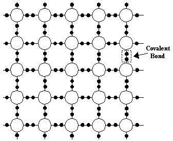
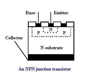
The Discovery of the PN Junction In 1939 Russell Ohl was studying crystals at Bell labs in the USA. Crystals were used as detectors in radio receivers and were notoriously unreliable. He thought that if he could produce a very pure form of silicon it could be developed into a very useful diode. After producing silicon that was 99.8% pure he still found that some of his diodes were as bad as the old cat'’ whisker. He started to examine one specimen that had a crack in the middle. He decided to measure the current flowing on each side of the crack and discovered that the current was affected by light. In fact it was the light itself that was causing the current to flow in the first place. On further inspection he found that the crystal had different levels of purity on each side of the crack and that the extra elements caused one side to have an excess of electrons, and the other side a deficit. Since opposites attract, electrons from one side had migrated to the other side to create a thin barrier of excess charge along a part of the crack. This barrier allowed electrons to travel in only one direction across it. When light shone on the crystal, its energy allowed electrons to move around. As they could only move in one direction an electric current flowed through the crystal. Walter Brattain who was a research physicist at Bell labs, saw Ohl’s work and realised that it could lead to a solid state alternative to the thermionic valve. He began working on semiconductors and was having some success, but had only managed to produce devices with a tiny amount of amplification. On 17th November 1947, he was working in his lab on the latest device, and kept having problems with condensation forming on the surface. To remove the condensation he placed the device under water and found to his amazement that the amount of amplification dramatically increased. He showed the device to John Bardeen and they began experimenting with different materials and electrolytes in an attempt to produce a device with a useful amount of amplification. They obtained good results with germanium and in December 1947 they produced the first point contact transistor. This was done by wrapping a strip of gold foil around part of a plastic triangle, cutting through it at one of the points and placing the point in contact with the germanium. The signal was put into one of the gold contacts and the output was taken from the other. The device worked extremely well and was the world’s first solid state amplifier. Several of the new germanium devices were made, but results were variable and the output from the device included a lot of noise. Early in 1948 William Shockley began work on a different concept that hopefully would overcome these problems. His work led to the development of the junction transistor. By April 1950 he had produced a working NPN germanium device. This could only work with low frequencies, but by early the following year most of these problems had been overcome, and in July the world’s first efficient junction transistor was announced, in a press conference. In 1956 Walter Brattain, John Bardeen and William Shockley shared the Nobel prize for physics for their invention of the transistor. The Junction Transistor Most modern transistors are made of silicon, which in its normal form is an excellent insulator. Silicon atoms form a crystal lattice, where the individual atoms are bonded together by sharing the outer electrons. This is called covalent bonding, where each individual atom shares its valence electrons with those of its nearest neighbours, by establishing electron pairs.
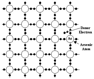
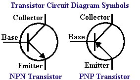
A silicon atom has 14 electrons with 4 outer or valence electrons. The silicon lattice can be changed from an insulator to a semiconductor by adding a tiny number of other atoms with either 3 or 5 valence electrons. This technique is called doping and only around 1 atom of the doping substance is added for every 100,000,000 atoms of silicon. If the doping substance is arsenic, which has 5 valence electrons, the lattice has an extra electron and produces N-type material.
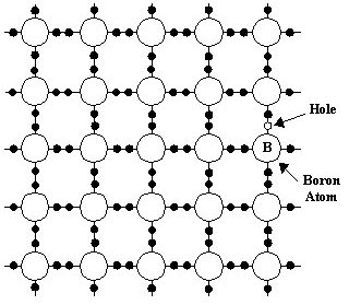
If the doping substance is boron, which has 3 valence electrons, the lattice has one electron missing. This is known as a hole and produces P-type material.
In N-type silicon the extra electrons are free to move and so can act as current carriers. This makes the material more conductive than normal silicon. In the P-type material the holes exert a considerable force of attraction for any free electrons and so they enable a current to flow.
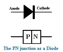
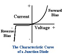
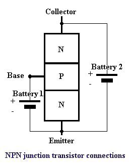
At the junction, electrons from the N-type will migrate into the P-type, and holes from the P-type will migrate into the N-type, within an area known as the depletion region. This produces a potential across the junction of about 0.7 Volts, with the N material being positive and the P material being negative. In practice this cannot be measured as there is no net current flow.
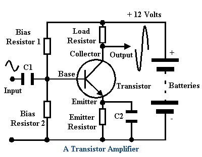
The Transistor Amplifier
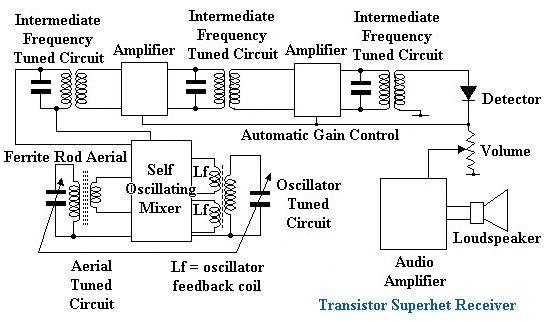
The large change in collector current compared with the tiny change in base current depends upon the current gain of the transistor. Typical values of current gain are between 50 and 500. A Transistor Radio Receiver Transistor radios are usually superhets, which provide high sensitivity with good selectivity.
The superhet uses a self-oscillating mixer, or frequency changer as its also called, to convert any aerial signal to a fixed frequency. This is done by mixing the aerial signal with the signal from the oscillator. When the two are combined in the mixer, it produces the original signals plus their sum and difference frequencies. When a station is tuned in, the oscillator frequency is also adjusted so that the difference in frequency between it and the tuned frequency is always the same. This gives a constant difference frequency which can be easily amplified, and by using suitable tuned circuits its bandwidth can be precisely set so that the receiver is very selective. The difference frequency is called the intermediate frequency, or I.F. frequency for short. After amplification the I.F. goes to the detector to obtain the original speech or music. The detector also provides a positive voltage that is used to control the overall gain of the receiver. It is called the 'automatic gain control' or AGC for short. The stronger the signal, the greater the voltage will be, and the gain will be reduced accordingly. The audio output from the detector goes to the volume control, and to the loudspeaker via the audio amplifier. The ferrite rod aerial appeared at about the same time as the transistorised receiver. It concentrates the electromagnetic field from the radio transmission, in the aerial coil and is very sensitive. The arrival of the transistor and the ferrite rod aerial, meant that for the first time, highly sensitive receivers could be very small, and use very little battery power.
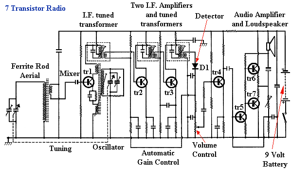
Circuit Description The signal from the ferrite rod is coupled into the self oscillating mixer, tr1. The oscillator section consists of a tuned transformer, with feedback windings in the collector circuit of tr1, and the emitter circuit of tr1. The mixer output is tuned to the I.F. frequency by the first I.F. tuned transformer, amplified by tr2 and tr3 and fed to the detector by the last I.F. tuned transformer. The positive output from the detector, D1, provides the automatic gain control voltage for the I.F. amplifiers, and the detected audio signal, that goes to the volume control, via a filter to remove the carrier signal. The output from the volume control goes to the first audio amplifier tr4 and to what is called a complementary push-pull amplifier, that consists of tr5, tr6 and tr7. The first transistor, tr5, drives the complementary pair, tr6 and tr7, which consists of an NPN transistor and a PNP transistor. The two transistors conduct on alternate half cycles of the audio signal. This type of amplifier provides low distortion and low current consumption, and can be physically very small as no transformers are required. This circuit is typical of many radios.
|